
1. Nontechnical Background
FPGAs or Field Programmable Gate Arrays are wonderful microchips, that allow for arbitrary logic circuit design at the hardware level. They can be programmed to do any kind of digital processing that you can think of.
Consider that NASA likes to use them, because they can be reprogrammed live – say on a satellite, and reconfigured to potentially fix errors or faulty hardware.
They became well known in 1997 for creating an efficient sound recognition device using genetic algorithms that ‘learned’ what circuit designs worked best.
Consider that you can reuse an FGPA to be something as simple as a signal invertor, sensor trigger, or multiplexor, all the way up to recreating a modern CPU such as the Amtel chip found in Arduinos. So yes, FPGAs can do anything a microcontroller can do, and more, if you have a large enough microchip. Unlike traditional microcontrollers and CPUs, FGPAs can be massively parallel, and run without a system clock.
We are introducing the Fipsy FPGA as a lightweight way to learn about FPGAs with a low cost, and learning materials targeted at Makers.
You have the potential to have a more efficient and real-time processing solution than you could achieve with microcontrollers. This is why FPGAs are commonly used for signal processing, such as audio and video signals, which have lots of data that needs to be crunched real-time.
Learning FPGAs is an ‘in’ to a world of custom hardware design. We can help you learn Verilog, a Hardware Description Language with syntax similar to C.
2. Design Concepts
Image you are working with a black box, and you don’t care how it works on the inside. You only care that you give it inputs, it does some ‘magic’ and delivers the proper output. The concept of black box design is central to Hardware Description Languages. In Verilog, the black boxes are modules, which you can think of as standard microchips:

You will notice that each module has a pre-established number of pins. These pins can act as inputs or outputs.
In reality, inside the black box, of course there are circuits that represent logic gates and logic pathways:
 But we don’t care about those, yet. We are building up a circuit by linking modules together, and it is only the inputs and outputs of each module that we have to care about!
We should focus on a block diagram of major functional units of our design, without getting into the nuance of how each module works. However, the inputs and outputs of the module should be a consideration:

Consider that everything uses this black box, and at the end of the day, the above design is just the internals of another black box:
A Full FPGA Design

What this means, is that a full FPGA design, is just another module.

Modules are great! They are reusable black-boxes. Each module can be reused again and again anywhere (just like if you said, hey I’m designing a motherboard and I want another ram module, and another, and another… let me just add one more).
Any module can use any other module, as long as the inputs and outputs are satisfied.

For those of you familiar with Object-oriented Programming, modules are kind of like being able to re-use an object description multiple times. Again, we love our black-box design. It allows us to remain very abstract and systems-design focused, before digging into the nuance of each module.
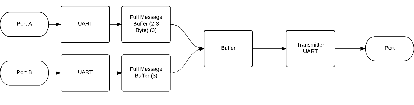
Here is an real example of a module flow diagram we used in our project, to capture the concept of MIDI digital signal merger. In merging two signals, of the same type, we where able to instantiate two UART modules that acted as message receivers, one for each port. Adding a third port would be trivial, since the UART receiver module was already declared.
We strongly encourage you to check out the FPGA Module schematics used by Michael Duerinckx in his Yearproject: FPGA MIDI synth
When you design for an FPGA, you will be developing a hierarchical set of modules. Relevant modules are interconnected – inputs and outputs. The module that no other module calls is inferred to be the top-most module.
The configuration of each module is then written in a Hardware Description Language (HDL) – of which Verilog and VHDL are common. We will do our examples in Verilog, because it has the more familiar C-like syntax. This can be confusing though because of this major nuance:
Hardware Description Languages describe an instantaneous configuration (of logic gates), all implemented at once! Lines of description language, are not sequential sets of instructions!
If you declare on line 1000
1 | reg [1:0] my_memory_register = 2'B01; //That means an array of binary memory that is 2 bits long, with an initial value of 01 |
and on line 2 have:
1 2 3 4 | if(my_memory_register == 2'B01) begin //More Configuration Code Here end |
The if statement will still validate as true. The purpose of HDL is to declare configurations of hardware, not to execute sequentially.
There are ways of encapsulating code into blocks, and ways of ensuring some things are done sequentially, but those are special cases. The default case is that all code is executed in parallel and at the same time. You are not writing code – you are establishing a configuration.
Return to the Wiki Overview