
Find the code for this example on GitHub.
The default blinky example is great, but most blinky examples operate at 1 Hz, or, 0.5 seconds on, and 0.5 seconds off. This is a picture of the default blinky example:
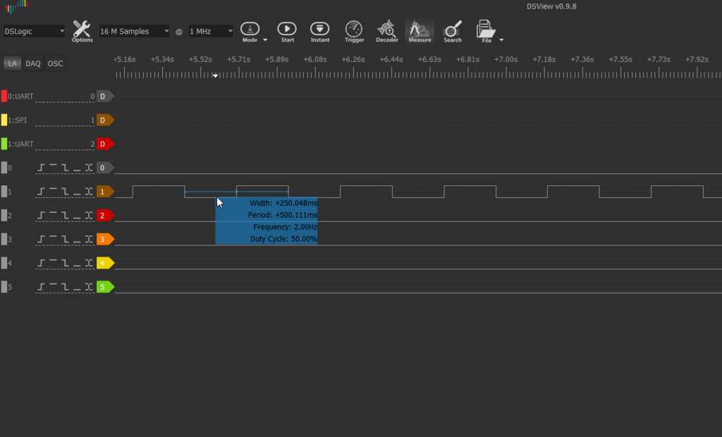
Our last example, Blinky operates at about 2Hz, which is really two cycles per second, each cycle having an on and an off phase that is 0.25 seconds long. So ONE way to get to 1Hz, is to trigger a state change on every other signal.
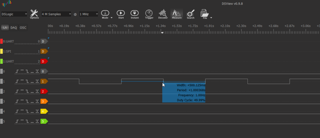
This is an example of what we want to build:
Our code is largely the same as before, except now we have:
1 2 3 4 5 6 7 8 9 10 11 12 13 14 15 | // View the signal on a chosen pin assign PIN20 = Out2Hz; // Also put the oscillator signal itself on a pin assign PIN11 = INTERNAL_OSC; reg flop1 = 1'b0; reg flop2 = 1'b1; always @ (posedge Out2Hz) begin flop1 <= flop2; flop2 <= flop1; end assign LEDn=flop2; |
First we set up registers ‘flop1’ and ‘flop2’, to be 0 and 1 respectively. This is their state at power-on, after the configuration is initialized.
Next we encounter:
1 2 3 4 | always @ (posedge Out2Hz) begin .. end |
This means that a set digital logic steps is run each time Out2Hz fires (which is a clock signal we generated previously in Blinky). Specifically, the events are fired on the positive edge of the clock signal. You could also trigger events at the ‘negedge’ of the clock signal. In the wild, posedge is much more common.
Consider that you can fire at the start, or end of clock tick as specified:
 A clock is a funny thing in Verilog. It MIGHT mean something connected to an actual digital oscillator (like CPUs have), but often it means act as a trigger when something happens.
Eg.
1 2 3 4 5 6 7 | always @ (posedge state_change_trigger) begin ... end |
So you could be monitoring a digital signal, and you only want to do something when it goes from 0 to 1 (positive edge), then you could use an always block.
Much more common you will see:
1 2 3 4 5 6 7 | always @ (posedge clock) begin ... end |
This is what you would do if you want to recreate a CPU with an FPGA, as in execute a set of instruction on each clock tick. Doing something at each clock tick, along with counters and registers, allow you to have some concept of time.
The statements inside the block always execute at each occurrence of the clock signal (specifically the positive edge of it, in our example).
Now what you have inside the always block is:
1 2 | flop1 <= flop2; flop2 <= flop1; |
Consider that the Verilog file would work JUST as well if we switched the order to:
1 2 | flop2 <= flop1; flop1 <= flop2; |
If flop1 was 0, and flop2 was 1, then after one clock tick, flop1 is 0 and flop2 is 1.
What you are doing is swapping the values with each other RIGHT at the moment of posedge for each clock tick. In Verilog, the order of statements does not matter, as you are describing a configuration of logic gates, not a program.
Now there is an exception to the fact that statements won’t execute in order, and that is if you use the following form of assignment:
1 2 | flop2 = flop1 flop1 = flop2 |
This may not work how you initially expect however:
If flop1 was 0, and flop2 was 1, then after one clock tick, flop1 is 0 and flop2 is 0.
Since they are executed in order, it works out that:
flop2 = flop1 //flop1 is 0 initially, so now flop2 is 0 (immediately, not later)
flop1 = flop2 //flop2 already has a 0 value, and you are declaring flop1 to be that state, immediately and in order
Consider that you want to use the <= when you want every change to happen at once, and in particular if you want to preserve the value of a variable till the ‘upcoming posedge’ execution state (as when we want flip1 and flop2 to be meaningful values after that <= until the instantaneous transition occurs).
Use = when logic by necessity must be sequential. Consider a design guideline that using = is a crutch or a handcap, and should be avoided. Most often there is a more “Verilog” way of accomplishing something rather than a series or =. You have to break out of the habit of designing a configuration as if you where writing executable code with a programming language. Usually a state machine, or counter is a better option.
The end of our example is then clear:
1 2 3 4 5 6 7 | always @ (posedge Out2Hz) begin flop1 <= flop2; flop2 <= flop1; end assign LEDn=flop2; |
We switch 1 and 0 states on flop 2 once each clock cycle. Since Out2Hz fires twice per second, flip2 lands on the 0 value once a second. Meanwhile, the LEDn is assigned to flop2, turning the LED on each time flop2 is 0 (driven to ground).
Full code is:
1 2 3 4 5 6 7 8 9 10 11 12 13 14 15 16 17 18 19 20 21 22 23 24 25 26 27 28 29 30 31 32 33 34 35 36 37 38 39 40 41 42 43 44 45 46 47 48 49 50 51 52 53 54 55 56 57 58 59 60 61 62 63 64 65 66 67 68 69 70 71 72 | /* Blinky_Rate_Divider.v */ module MakeFPGA_Top( PIN7, PIN8, PIN9, PIN10, PIN11, PIN12, PIN13, PIN14, PIN17, PIN18, PIN19, PIN20, LEDn ); // Define all of the above pins as available for general I/O inout PIN7, PIN8, PIN9, PIN10, PIN11, PIN12, PIN13, PIN14, PIN17, PIN18, PIN19, PIN20; // Except the LED, which is only an output, for which driving low lights the LED output LEDn; // At this level, all named signals are wires wire PIN7, PIN8, PIN9, PIN10, PIN11, PIN12, PIN13, PIN14, PIN17, PIN18, PIN19, PIN20, LEDn; // Instantiate a connection to the internal oscillator wire INTERNAL_OSC; // IMPORTANT - This oscillator has very poor accuracy - do not depend on it for critical timing. defparam OSCH_inst.NOM_FREQ = "2.08"; // Must be one of the allowed frequencies (2.08MHz default) OSCH OSCH_inst( .STDBY(1'b0), // Enable input, 0=Enabled, 1=Disabled (also disabled if Bandgap=OFF) .OSC(INTERNAL_OSC), // Set the oscillator output to appear on the wire defined above .SEDSTDBY() // This output is not required for normal use ); // BASELINE EXAMPLE // Create wires to connect the counter (see example application) wire Out2Hz; /* Default assignments - If pins are not used, it may be a good idea to drive them to a known state. */ assign PIN7 = 0; assign PIN8 = 0; assign PIN9 = 0; //assign PIN10 = 0; //assign PIN11 = 0; assign PIN12 = 0; assign PIN13 = 0; assign PIN14 = 0; assign PIN17 = 0; assign PIN18 = 0; assign PIN19 = 0; //assign PIN20 = 0; //assign LEDn = 0; // Instantiate the counter/divider FreqDiv20Bit FreqDiv20Bit_inst( .CLOCK(INTERNAL_OSC), // Drive with internal oscillator .RESET(PIN10), // Reset when chosen reset pin is high .MSB(Out2Hz) // We expect 2 Hz out with 2MHz in ); // View the signal on a chosen pin assign PIN20 = Out2Hz; // Also put the oscillator signal itself on a pin assign PIN11 = INTERNAL_OSC; reg flop1 = 1'b0; reg flop2 = 1'b1; always @ (posedge Out2Hz) begin flop1 <= flop2; flop2 <= flop1; end assign LEDn=flop2; endmodule |
1 2 3 4 5 6 7 8 9 10 11 12 13 14 15 16 17 18 19 20 21 22 23 24 25 26 27 28 29 30 31 32 33 34 35 36 37 38 39 40 41 42 43 44 45 46 47 48 49 50 51 52 53 54 55 56 57 58 59 60 61 62 63 64 65 | /* FreqDiv20Bit.v This module implements a 20-bit counter with only the most significant bit provided as an output. In effect, this is a frequency divider for which the output toggles at a rate equal to the clock frequency divided by 2^20. The clock is an input and is applied to the sequential logic clock. Technically, the output is not a clock within the FPGA, but a logic signal, although it will toggle like a clock. There is a reset input that will set the count to zero on each clock edge for which it is set (logic high). This reset will clear the output to logic low, and the count and output will remain that way as long as reset is active. The reset input can therefore be used to stop the output signal from toggling at an unpredictable point in the cycle. More complex logic could be developed to provide a more predictable control. */ //----------------------------------------------------------------------------------------------- // Module header with identification of connected signals //----------------------------------------------------------------------------------------------- module FreqDiv20Bit(CLOCK, RESET, MSB); input CLOCK; input RESET; output MSB; //----------------------------------------------------------------------------------------------- // Signal definitions, registers, variables //----------------------------------------------------------------------------------------------- // Signal types for I/O wire CLOCK; wire RESET; wire MSB; // Internal count bits reg [19:0] count; //----------------------------------------------------------------------------------------------- // Module logic definition //----------------------------------------------------------------------------------------------- // 20-Bit counter with synchronous reset // With reset not in the sensitivity list, the reset is synchronous (on next clock edge) // If reset were in the sensitivity list, the reset would be asynchronous, which might // not be supported by the tool or the underlying hardware of the chip or both // Without specifying bits and bit sizes of constants and variables, all defined bits are used. // The tool logic synthesizer will warn that constants are 32-bit by default and it has // to work out the impact for you. Yet writing it like this makes the code easier to // understand in this simple example. always @(posedge CLOCK) begin if(RESET) count <= 0; else count <= count + 1; end // Connect the output assign MSB = count[19]; //----------------------------------------------------------------------------------------------- // End of module //----------------------------------------------------------------------------------------------- endmodule |
Return to the Overview